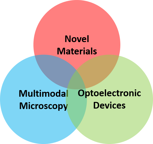
The KahmannLab stands on three broad legs, which are our fields of expertise. Synthesis of (solution-processed) novel materials and their development/optimisation goes hand in hand with in-depth photophysical characterisation and a special attention to local information enabled through optical microscopy. We love light-matter interactions and everything that emits or absorbs light.
Ultimately, the expertise on materials and photophysics works in concert to design, characterise, and to improve the performance of optoelectronic devices. Boosting our capabilities by means of computational approaches is a further central concern of our strategic work.
As such, we work on the boundaries of classical disciplines, such as physics, chemistry, materials science, and electrical engineering. Benefitting from diverse scientific backgrounds and experimental skill sets is at the heart of the KahmannLab’s philosophy.
Our Areas of Expertise
Photophysics & Microscopy
What happens when materials absorb light? How fast do they emit light and at what energy? How is this affected by processing conditions? And what can we learn from looking at these aspects under the microscope?
Photoluminescence spectroscopy and microscopy in all their facets are our dearest experimental techniques. We study the interaction of light with matter to discover new properties or to understand exciting phenomena encountered in new compounds.
We particularly care about dynamic processes, such as recombination and diffusion of excitations, as well as the spatial correlation of different signals. Developing computational approaches for smarter analysis are an important concern to treat these large data sets.
Novel Materials
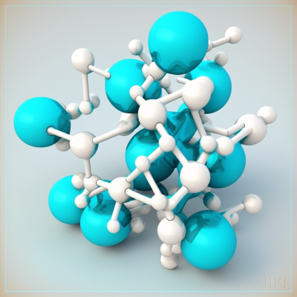
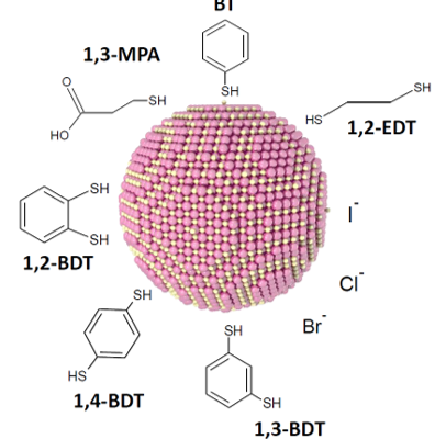
We love semiconductors & in particular those processed from solution. Our work considers organics compounds, (e.g. conjugated polymers & small molecules), inorganic compounds, (colliodal nanocrystals), or hybrid compounds (halide perovskites).
Intricate structure-property relationships and how they can be tailored, for example, through interaction of organic and inorganic building blocks, is a key objective of our work. Emission of polarised light or anisotropic transport of charge carriers are two examples of important properties that can be tuned in such a way.
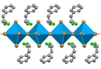
At the moment, we are particularly interested in the class of low-dimensional halide perovskites, whose electronic dimensionality can be manipulated through the intelligent choice of spacer molecules.
Optoelectronics
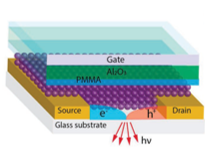
Optoelectronic devices are key building blocks of modern society. Whether it is to harvest sunlight for electricity production or to inject an electric current for light emission, we are keen to study, tailor, and optimise the performance of devices, such as solar cells, light-emitting diodes, and photodetectors.
Much of our research is driven by the goal to create a more sustainable society – we aim to contribute to the quest for better-performing and longer-lasting solar cells, as well as more efficient ways to transform electrical energy into light. A central approach in our lab is to study these devices under operating conditions using our microscopy and specroscopy set-ups.
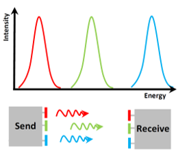
A further key project is to create pathways to exploit our versatile materials systems for future optical communication platforms, such as through visible light communication.
Impressions from the Lab
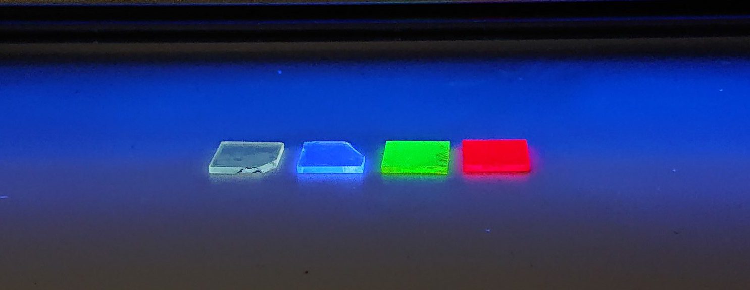
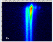
Light-Induced Filaments on a Tin-Based Perovskite
Electrical Pulsing and Trigger Signals
Notes and Sketches
Second Harmonic Generation
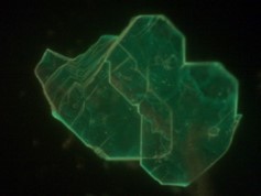
A Wide-Band Bap Perovskite
MAPbBr3 Nanowires
Controlled Atmospheres
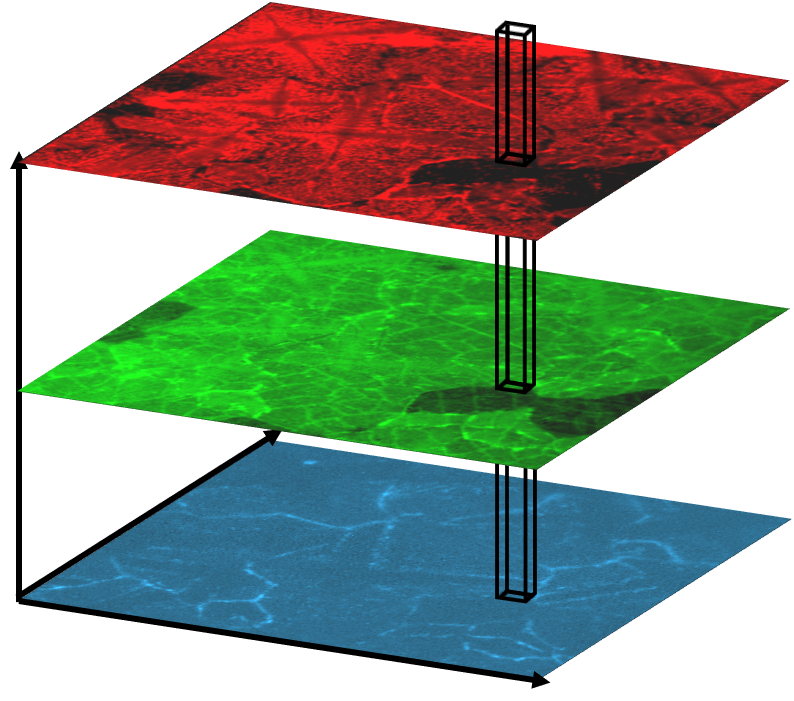
Cryo-Measurements on the Hyperspectral
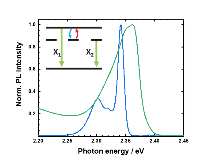
Narrow & Broad Emission Bands
Time Resolved PL Spectra
Luminescent Perovskite Nanocrystals
Our Equipment
We have access to a broad range of experimental techniques and facilities in collaboration with the Optics and Photonics of Condensed Matter and the Semiconductor Physics groups. This includes wet chemistry facilities for synthesis and sample preparation, a nitrogen glovebox with a spin coater, and thermal evaporators.
The wide environement of the Institute of Physics provides a multitude of relevant characterisation techniques, e.g. X-ray diffraction, electron microscopy, circular dichroism spectroscopy, and Raman spectr-microscopy.
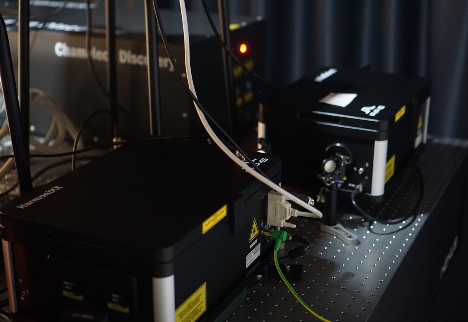
Femtosecond laser System
Coherent Chameleon Discovery
The Chameleon is a powerful broadly tuneable (660-1320 nm) laser source that emits pulses of around 100 fs duration at 80 MHz repetition rate and up to 4 W. We use a pulseSelect pulse picker from APE to reduce the repetition rate (down to 310 Hz) and a HarmoniXX second harmonic generator to cover wavelengths down to 330 nm.
Optical Microscope
Evident IX73
The heart of our microscopy lab is a manual IX73 inverted microscope from Evident. Beam shaping enables us to use the platform both for focused and for wide-field microscopy using LEDs and the femtosecond laser. The system is directly coupled to our spectrometer, but uses an internal steady-state camera to image samples both in real an in k-space (Fourier imaging).
Multi-Purpose PL Set-up
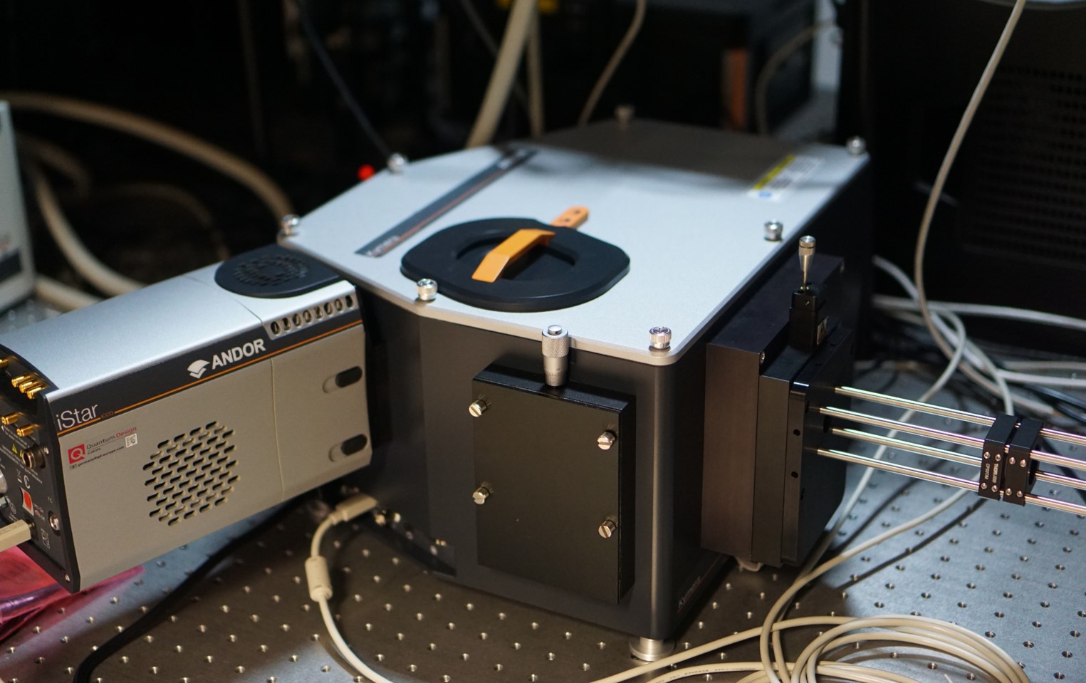
Kymera 328i + iStar
The Kymera is an imaging spectrograph directly coupled to our optical microscope – equipped with three gratings and one mirror, we are able to measure spectrally or spatially resolved emission from the microscope’s sample plane with a time-resolved iCCD camera (2 ns resolution) in the visible spectral range. An alternative beam path enables macroscopic measurements bypassing the microsocpe.
Angular EL & PL Test
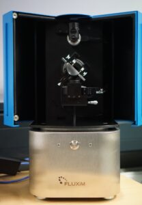
Fluxim Phelos
The Phelos is a goniometer-based spectroscopy set-up dedicated to tracking the angle-dependence of the luminescence emitted from thin films upon photoexcitation or from light-emitting devices after electrical injection.
Our Funding
DFG — Weave Lead Agency Scheme
Singlet and triplet energy transfer In two-dimensional hybrid perovskites (INTENSITY)
2025-2028
European Fund for Regional Development
Modern light-emitting diodes and organic solar cells: new pathways towards a more sustainable production and use of energy (Nachleuchten)
2024-2027
DFG Major Research Instrumentation Programme
Femtosecond laser spectro-microscopy system
2024
Leverhulme Early Career Fellowship with Matching Funding of the Isaac Newton Trust
Hybrid nanostructures for chiral optoelectronics – polarising communication